


PRINTED CIRCUIT BOARD DESIGN AND DEVELOPMENT
We offer services of the qualified engineers in the PCB design and development of any complexity. We provide the full range of work – from planning to making prototypes and issuing design documentation for mass production.
It is possible to perform it in separate stages:
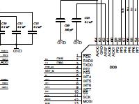
- concept creation of the device and circuit diagram development;
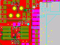
- PCB layout (tracing) on the circuit diagram;
- Making prototypes.
PCB layout is carried out in the modern packages. We trace PCB only manually. Automatic tracing cannot yet provide that quality which is necessary for complex multi-layer boards.
The cost and the due date of the finished work are estimated by the requirements specification, depending on complexity and labor intensity. It is usually required 2 to 4 weeks for PCB tracing; however the exact dates can be determined after requirements specification analysis.
To place an order for the design of the PCB you just need to give us the following: circuit diagram, the list of components, dimensional drawing (construct), and requirements for wiring, laying bus, and power supply plan.
Our specialist will contact you within 24 hours and specify the price and production period of your PCB.
After your PCB designing is done, you get all the initial information (PCB project file), files for PCB production, and, if necessary, a complete set of design documentation for PCBs, formalized by the Common System for Design Documentation or according to your personal requirements.